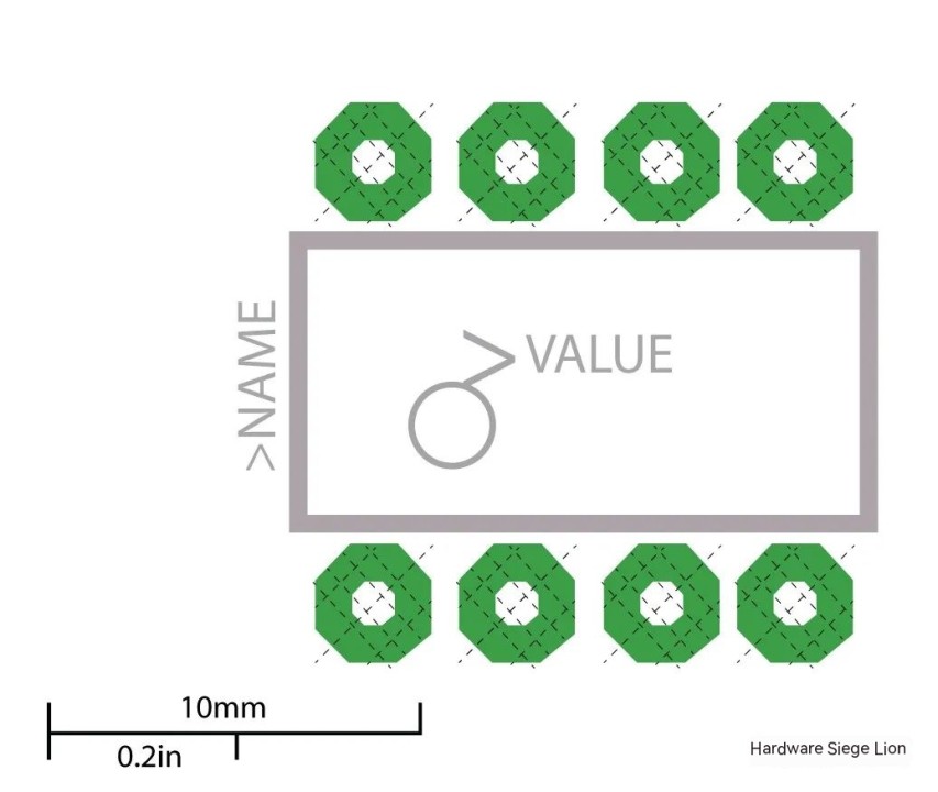
Details of test chip designs: pad pitch, layout, materials, and

By A Mystery Man Writer

Electronics, Free Full-Text
What is a Pad in PCB Design and Development
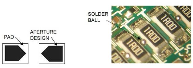
5 Key Design Features of an Effective Solder Paste Stencil
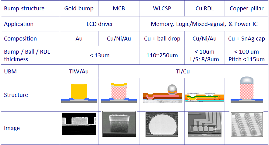
ChipMOS TECHNOLOGIES INC. – Back-end testing service for memory, LCD Diver, Bumping and MEMS.

A compute-in-memory chip based on resistive random-access memory
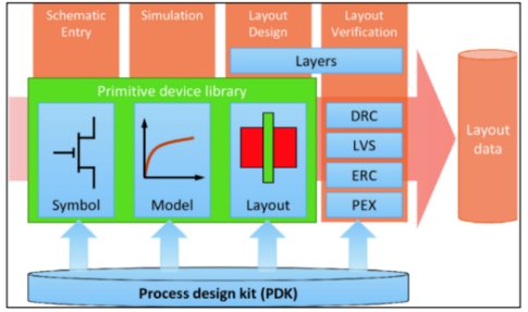
Understanding the Importance of Prerequisites in the VLSI Physical Design Stage

Changqing LIU, Loughborough University, Loughborough

RDL and Flip Chip Design
Advanced Packaging Part 2 - Review Of Options/Use From Intel, TSMC, Samsung, AMD, ASE, Sony, Micron, SKHynix, YMTC, Tesla, and Nvidia

Design and characterization of a copper-pillar flip chip test vehicle for small form-factor packages using 28nm ELK die and bump-on-trace (BOT)
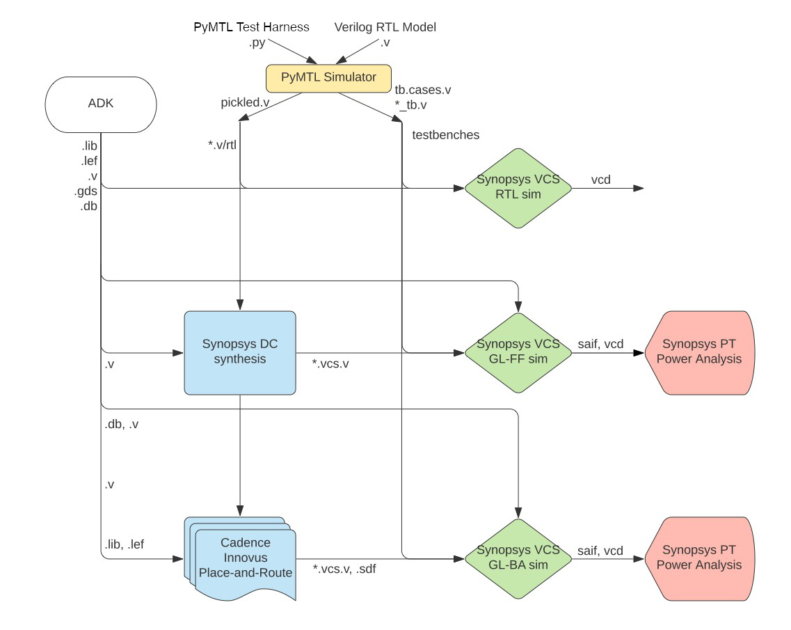
ECE 5745 Tutorial 4: Synopsys/Cadence ASIC Tools

Design guide - Mandalon EN

Changqing LIU, Loughborough University, Loughborough
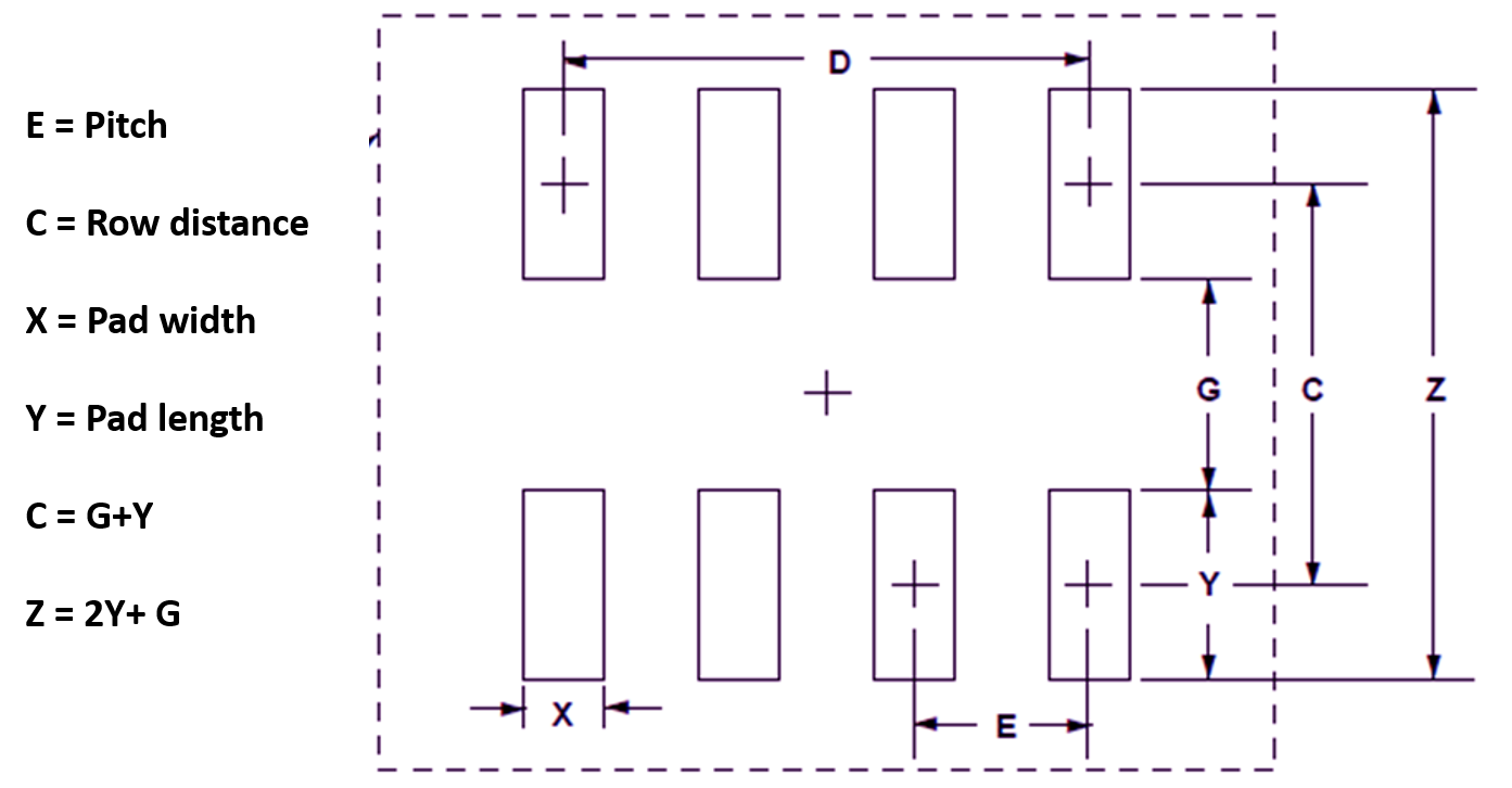
PCB pad design principles
- The Lymphedema Store
- Smilepad XXL Anion Air Sanitary Pads for Women | Anion Chip | Up to 10 Hrs. Long Protection | Combo Pack of 40 Pads

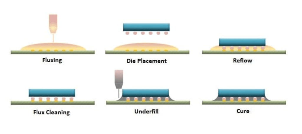
- Schematic of the chip/bump build-up cross-section.

- Chip Board « Fleenor Paper Company

- pcb - What is the pad size required for this BGA AW H3 Chip? - Electrical Engineering Stack Exchange