Thursday, Oct 03 2024
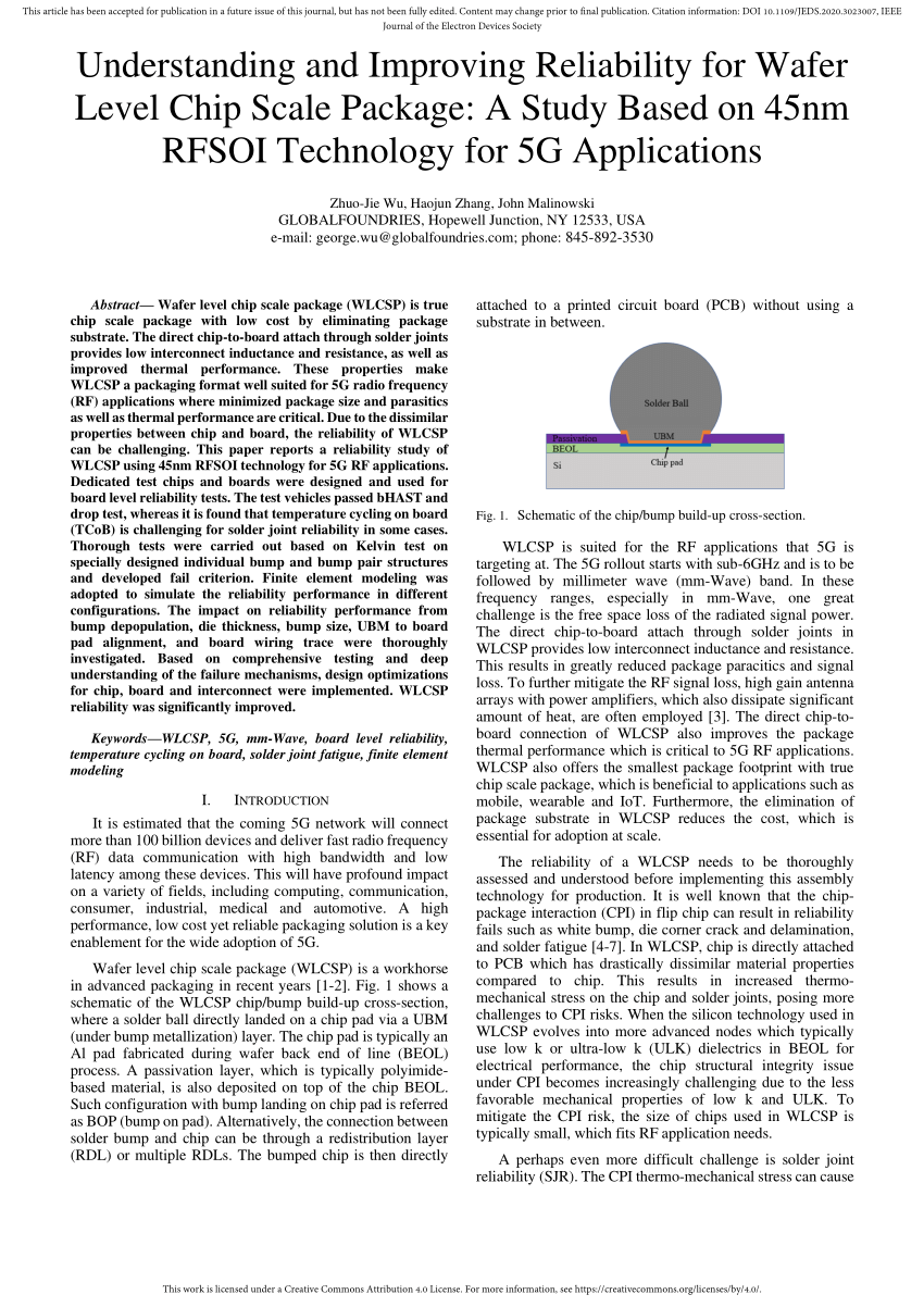
Schematic of the chip/bump build-up cross-section.

By A Mystery Man Writer
What Are Through-Silicon Vias?
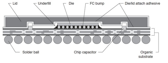
Faraday Technology Corporation-Flip-Chip Package

Advanced Flip Chip Packaging

State-Of-The-Art of Advanced Packaging

Chip Bonding - an overview

Solder Bump - an overview
PDF) Understanding and Improving Reliability for Wafer Level Chip

SEM image of a cross section of an unstressed 30 μm solder bump
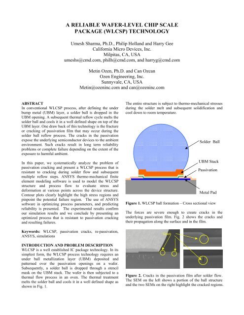
a reliable wafer-level chip scale package (wlcsp) - AKRO Engineering

Zhuojie WU Research profile

Schematics of flip-chip bump and UBM structure

Multiple System and Heterogeneous Integration with TSV-Interposers
Weibull plots for TCoB fails based 1000 ohms and 0.1 ohms
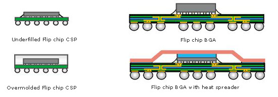
A Brief Introduction of BGA Package Types
Related searches


Related searches
- Kinetix Tennis on X: Congratulations to K2's student Dalia T. - a new Kinetix Tennis student standout at the club! Dahlia was runner-up at the Kinetix Tennis USTA tournament this weekend! #tennis #

- YOURS Plus Size Black Disco Leggings

- Women's Burton Avalon 2L Stretch Bib Pants (Short)

- Carhartt WIP Tapered Cargo Pants 'W' Collins Pant' in Beige

- Spine Injuries in Sports

©2016-2024, doctommy.com, Inc. or its affiliates