Wednesday, Jul 10 2024
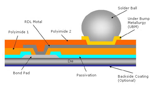
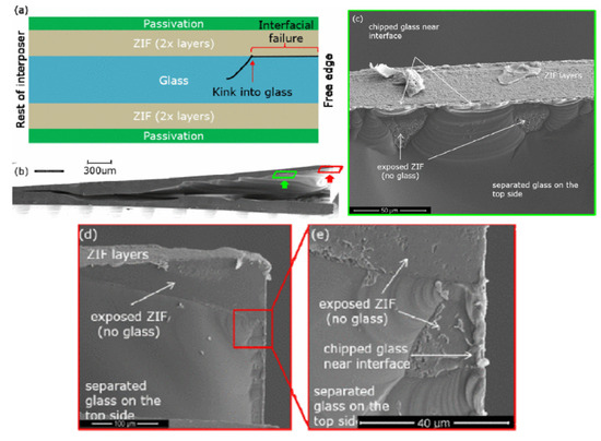
The bond pad redistribution layer (polyimide 1) and the under bump

By A Mystery Man Writer
Design Optimization of Pillar Bump Structure for Minimizing the

Materials, Free Full-Text
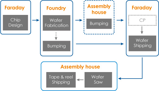
Faraday Technology Corporation-WLCSP Testing & Bumping Process
Faraday Technology Corporation-WLCSP Testing & Bumping Process

Warren FLACK, Vice President, PhD
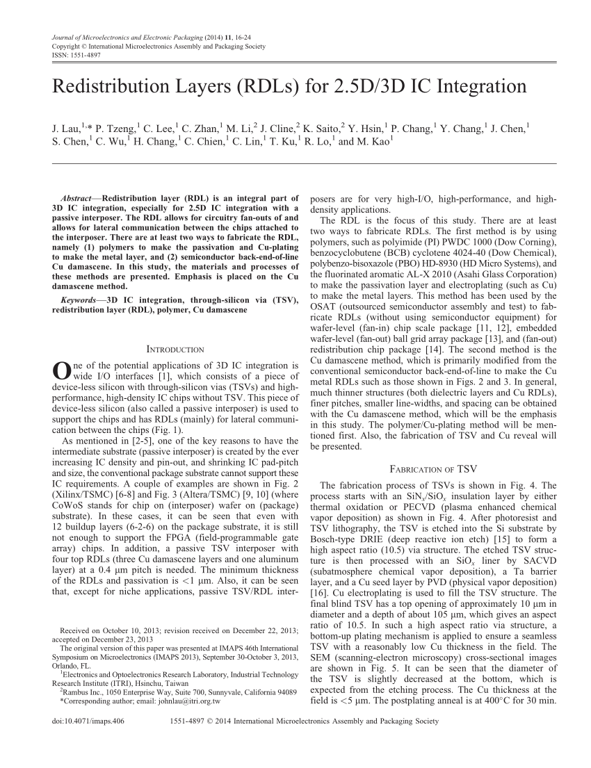
PDF) Redistribution layers (RDLs) for 2.5D/3D IC integration

Illustration of polyimide or LCP substrate and solder assembly

Polymers, Free Full-Text

Warren FLACK, Vice President, PhD

WO2018237377A1 - Curable polyimides - Google Patents

Recommended process application for the HD-8001 on 300 mm wafers
Polymers, Free Full-Text
Electromigration Performance Of Fine-Line Cu Redistribution Layer
Warren FLACK, Vice President, PhD
Related searches
- Bumps under your tongue? – The Island News – Beaufort, SC
- Lumps & Bumps - Cause for Concern?: Warrenton Dermatology & Skin Therapy Center: Board-Certified Dermatologists

- Bump in the Night VHS VCR Tape Mr Bumpy Tales From Under the Bed OOP Video 13131170030

- Best Maternity Jeans - Indigo – BAE The Label Australia

- Premium Under Bump Skinny Maternity Jeans

Related searches


©2016-2024, doctommy.com, Inc. or its affiliates