U-Bump Metalization - Tango
By A Mystery Man Writer
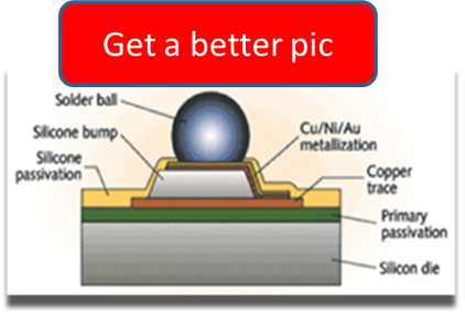
As the foundation of wafer bumping processing, the Under-Bump Metallization (UBM) stack must provide a strong, stable low resistance electrical connection to the IC’s pads and the surrounding

DSC curve of SnAg bumps Download Scientific Diagram
High Performance Electroless Nickel that's Lead and Cadmium-Free

PostPress May/June 2018 by petersonpublications - Issuu

The Seal Of Quality - A Riot Primer, Part 2 - Last Rites

Electronics, Free Full-Text

US8803338B2 - Semiconductor device having under-bump metallization

PDF) Pb-free Sn/3.5Ag electroplating bumping process and under

Music – Opinions

PDF] Under Bump Metallurgy (UBM)-a technology review for flip chip

A study in flip-chip UBM/bump reliability with effects of SnPb
SN74AVC4T234ZSUR & TXB0102YZPR - Under Bump Metallization (UBM
Tango Systems Inc. Achieves Conformal Deposition for 15:1

U-Bump Metalization - Tango
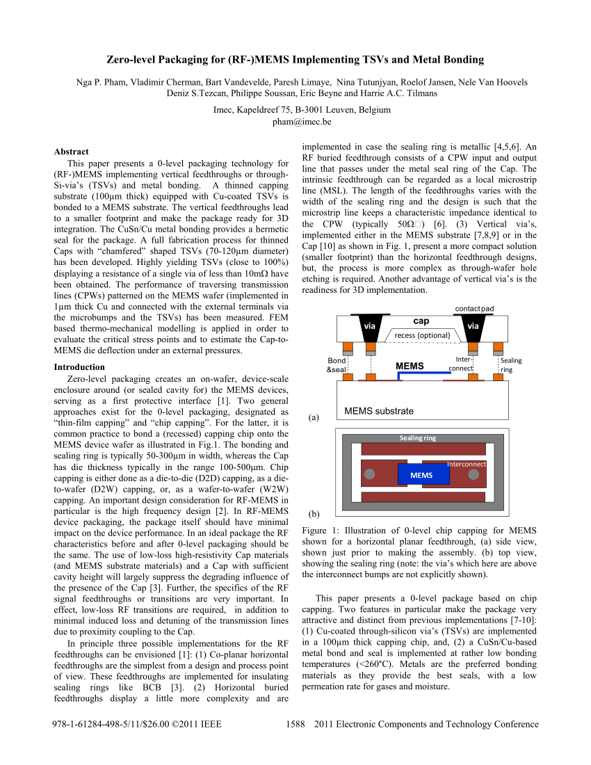
PDF) Zero-level packaging for (RF)MEMS implementing TSVs and metal

PC7457 by Microchip Technology Datasheet
- Hard lump under the skin: Causes and pictures
- CLiO Women's Seamfree Under the Bump Maternity Briefs 4 Pack - Multi

- 11 Types of Lumps, Bumps & Lesions Under Your Dog's Skin

- Motherhood MaternityWomen'sMaternity Bump Start 2 Pack Under Belly Casual Leggings, Black and Grey, Small : : Clothing, Shoes & Accessories

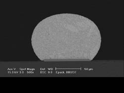
- Figure 3 from Under Bump Metallurgy (UBM)-a technology review for