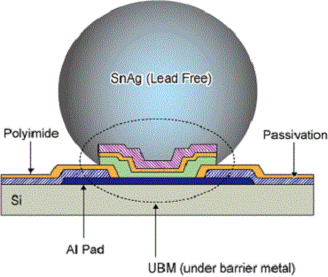
Bump on Pad, Wafer Process Technology
By A Mystery Man Writer
Bump on Pad Key features include: Wafer process and bumping in consolidated assembly. Technology supporting wide range of products from mobile devices to

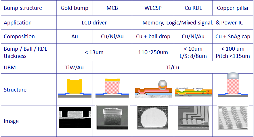
Semiconductor Back-End Process 7: The Wafer-Level Packaging
ChipMOS TECHNOLOGIES INC. – Back-end testing service for memory, LCD Diver, Bumping and MEMS.

Wafer Level Chip Size Package (WLCSP) Guidelines - EEWeb

Solder Bump Vertical Probe Cards Revolutionizing Semiconductor Testing by Semi-Probes Inc - Issuu

Prestige Popular Stainless Steel Pressure Cooker, Litres

InFO (Integrated Fan-Out) Wafer Level Packaging - Taiwan Semiconductor Manufacturing Company Limited
Illustration of double bump flip-chip process.
Prestige Popular Stainless Steel Pressure Cooker, Litres

Flip chip bumping technology—Status and update - ScienceDirect
Flip chip technology

Solder Bump - an overview


- Women Pantyhose Tights Leggings Woman Non Slip Stockings Short Socks - China Cotton Socks and Sport Socks price

- EHQJNJ Tankini Tops for Women Swimwear High Waisted Bikini Push up Two Piece Swimsuits Vintage Swimsuit Two Piece Retro Ruched High Waist Print Bikini

- Calça Legging Puma Essentials Feminina - Preto

- 6 Pair Invisible Clear Bra Straps Soft Transparent Replacement Bra Shoulder Strap Adjustable Women's Bra Straps Clips Non-slip Bra With Clear Straps F

- Black PU Leather Button Detail Leggings, Leather Leggings