A study of thermal cycling and radiation effects on indium and
By A Mystery Man Writer
The BTeV hybrid pixel detector is constructed of readout chips and sensor arrays which are developed separately. The detector is assembled by flip-chip mating of the two parts. This method requires the availability of highly reliable, reasonably low cost fine-pitch flip-chip attachment technology. We have tested the quality of two bump-bonding technologies; indium bumps (by Advanced Interconnect Technology Ltd. (AIT) of Hong Kong) and fluxless solder bumps (by MCNC in North Carolina, USA). The results have been presented elsewhere [1]. In this paper we describe tests we performed to further evaluate these technologies. We subjected 15 indium bump-bonded and 15 fluxless solder bump-bonded dummy detectors through a thermal cycle and then a dose of radiation to observe the effects of cooling, heating and radiation on bump-bonds. We also exercised the processes of HDI mounting and wire bonding to some of the dummy detectors to see the effect of these processes on bump bonds.

Tailoring lithium concentration in alloy anodes for long cycling

Why separation is needed in pharmaceutical multiple component

PDF] Characterization of indium and solder bump bonding for pixel detectors

Delafosse CHRISTIAN, Medical Doctor, Hospital Simone Veil, Montmorency, department of pneumology

Use of CCD for reflow process design

Applied Sciences, Free Full-Text

REHVA Journal Thermal impact of street canyon microclimate on the

AIT Dummy Detector Bump Daisy Chain.

HgCdTe Detector Chip Technology

High thermal conductivity in indium-based metal/diamond composites

A dual-mode textile for human body radiative heating and cooling

Fermin REYGADAS, Executive Director, PhD

Stud bumping for flip chip - An alternate strategy

Efficient semiconductor thermal management - News

Pushing the boundaries of photovoltaic (PV) technology
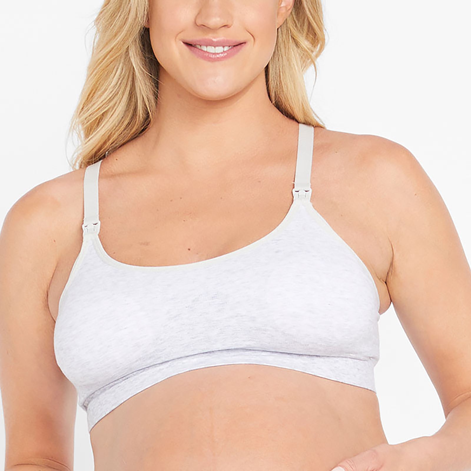
- Bonds Women's Originals Maternity Support Singlet - White

- Bonds Maternity Nursing Breastfeeding Pregnancy Bumps Seamfree
- Bonds Ladies Bumps Maternity Wirefree Bra sizes 10A 12A Colour Red Maroon

- Shop Bonds Womens Bumps Maternity Easyfit Tops Breastfeeding Clip Bra Purple Leopard - Dick Smith

- San Francisco Giants Barry Bonds, #25, bumps into Chicago Cubs

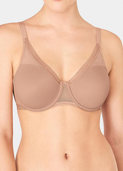
- Bali Women's Comfort Revolution Front-Close Shaping Underwire Bra

- Triumph Inifinite Sensation Underwired Minimiser Bra
- Skinny Fit Cargo Joggers

- Women's Sports Bodysuits Plus Size Seamless Plain Scoop Neck - Temu

- PSD Detail, The Amazing Spiderman, Official PSDs ❤ liked on Polyvore featuring avengers

- Body Wrappers Deep V Convertible Bra Adult 283 – Dance Essentials Inc.

- Frauen Sexy Hollow Out Fischernetz Strumpfhose Glitzer Strass Diamant Verziert Slim Mesh Strumpfhosen Durchsichtige Netzstrümpfe Party Clubwear

- Women's Athletic & Outdoor Sandals & Slides - Women's

- Pin on My Style

- Home Gym Ideas 2024
