Case study: 8 and 14-layer HDI with Stacked Vias

By A Mystery Man Writer
This case study focuses on the challenges and solutions that we implemented to design complex HDI boards with stacked vias.
Ball Grid Array (BGA) Breakouts, Second Edition
HDI Layer Stackup Design for Large Dense PCBs - Rush PCB
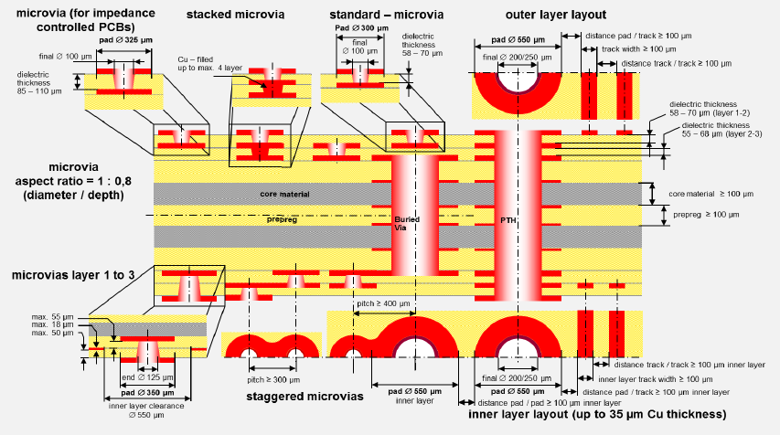
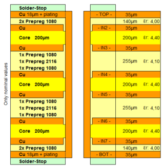
HDI board stack-ups – PCB HERO

Understanding Proper PCB Design (Part 2) - Circuit Cellar
a) SEM-micrograph of the top part of a 10 layer stacked via after

HDI PCB Design,Manufacturing and its cost

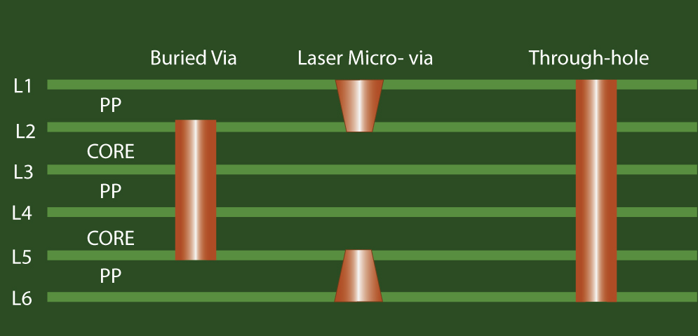
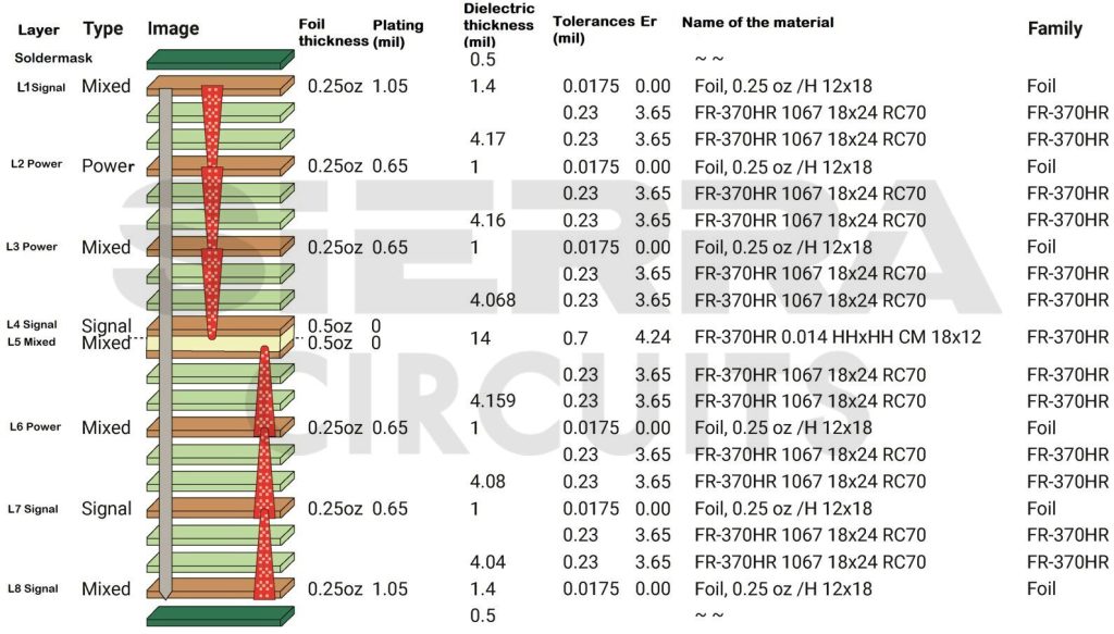
High-Speed PCB Design- Layer Stack-Up, Material Selection, and Via Types

HDI board stack-ups
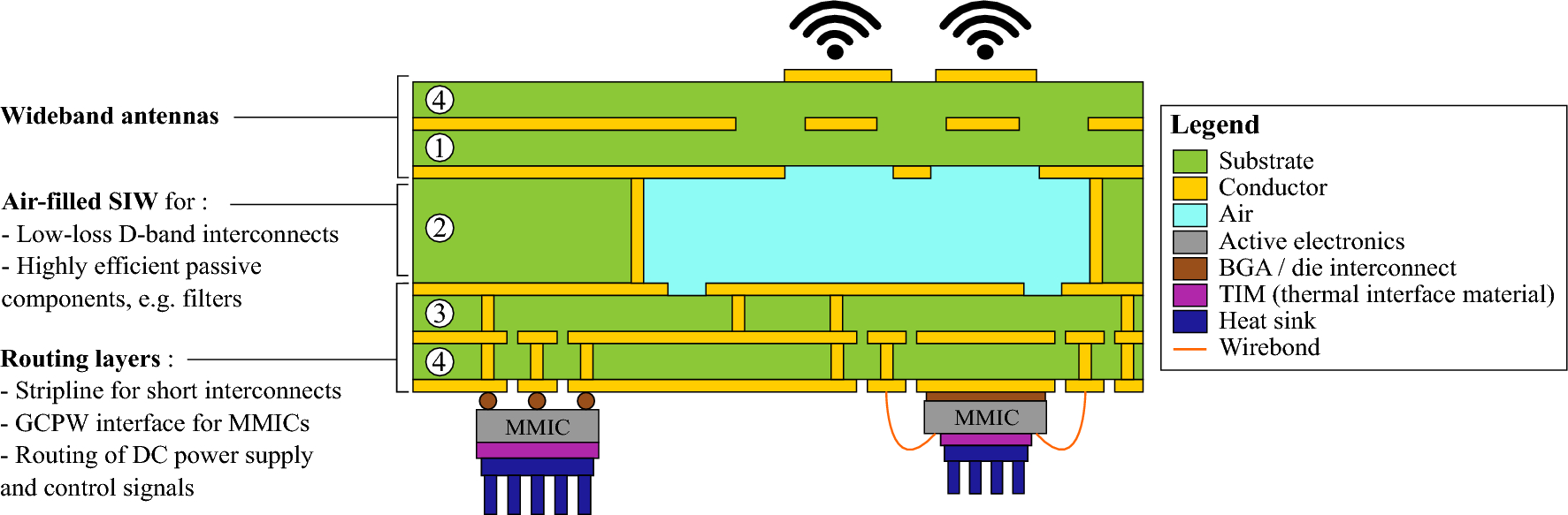
Air-filled SIW technology for mass-manufacturable and energy-efficient terahertz systems
Case study: 8 and 14-layer HDI with Stacked Vias

PCB Vias: An In-Depth Guide
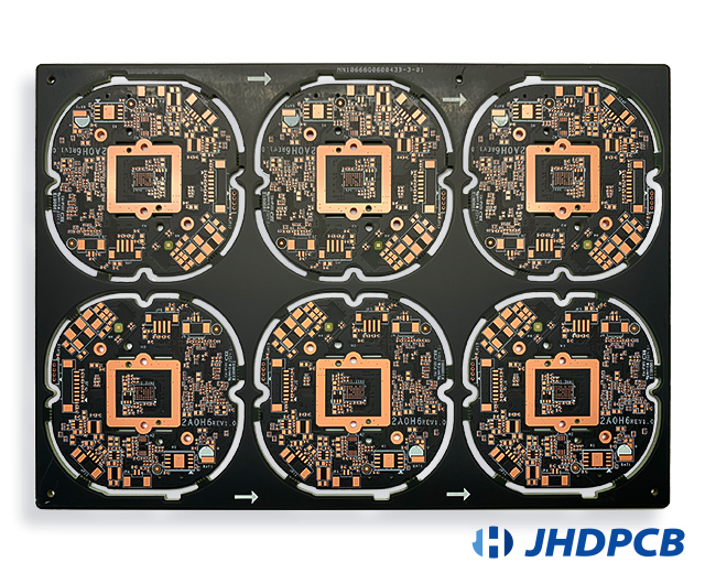
High Density Interconnect HDI PCB Manufacturer - Jhdpcb

Understanding Proper PCB Design (Part 2) - Circuit Cellar

HDI PCB Stackup - Venture Elctronics


- ASEIDFNSA Fuzzy Stacked Leggings Workout Top -Up Women'S Nine-Minute Jeans Super Bottom Coloured Pants Slim Pants Bomb Pants
- Vetinee Women's Slim Fit Stretch Jeans High Waisted Casual Slim Fit Denim Capri Pants Size XL

- Disney Girls Lilo & Stitch Clothing Set - Stitch Sweatshirt Hoodie, Shorts and Jogger - 3-Piece Outfit Set - Sizes 4-16 : : Clothing, Shoes

- Verified 10% Off SPANX Promo & Coupon Codes March 2024

- COTOWIN 1.25 Wide Thick Heavy Cotton Webbing,6 Yards (Natural White, 1.25“)
